Jane Street Challenge: Can You Reverse Engineer An ASIC?
Below is my solution to the Jane Street ASIC reverse engineering challenge.
I solved it on August 8, 2026 (three days after it was posted) and held off on publishing this until after submissions closed.
I see some of you on Hacker News were already posting solutions the morning of September 4, you rascals, submissions weren't even closed yet! This is also my way of pointing out that I am both an early solver and a woman of virtue, and I need you to know both of those things :P
To be fair, we were a little busy launching collusion.wiki, which hit #1 on Hacker News that same morning, and I was also marathoning a deadline at work, so please, by all means, you lot can have your Hacker News points, I need a nap.
August has been a sufficiently weird month.
Jess Solution
The premise of the challenge is as follows: we want to take the physical layout of a mystery chip and reconstruct a logical circuit from it. Once we reconstruct this logical circuit, we want to find an input to the circuit that makes the success signal go high. The answer we submit to the puzzle authors is the output emitted by the output generator once we find such an input.
The idea is that if we reconstruct the logical circuit correctly, then our answer would match the expected output when the success signal is asserted.
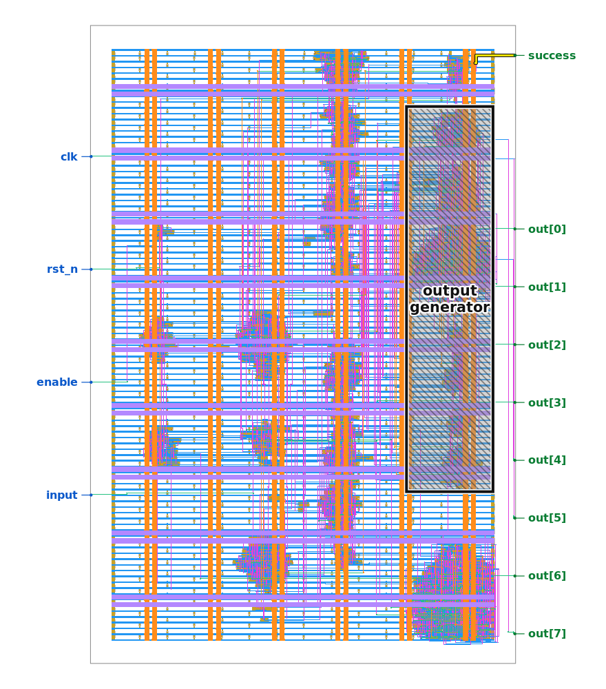 Figure from Jane Street asic-puzzle-2026.
What Are These Rainbow Rectangles?
At the start of the challenge, we are given a puzzle.gds. Coming from software, I had to begin by understanding what a .gds file was.
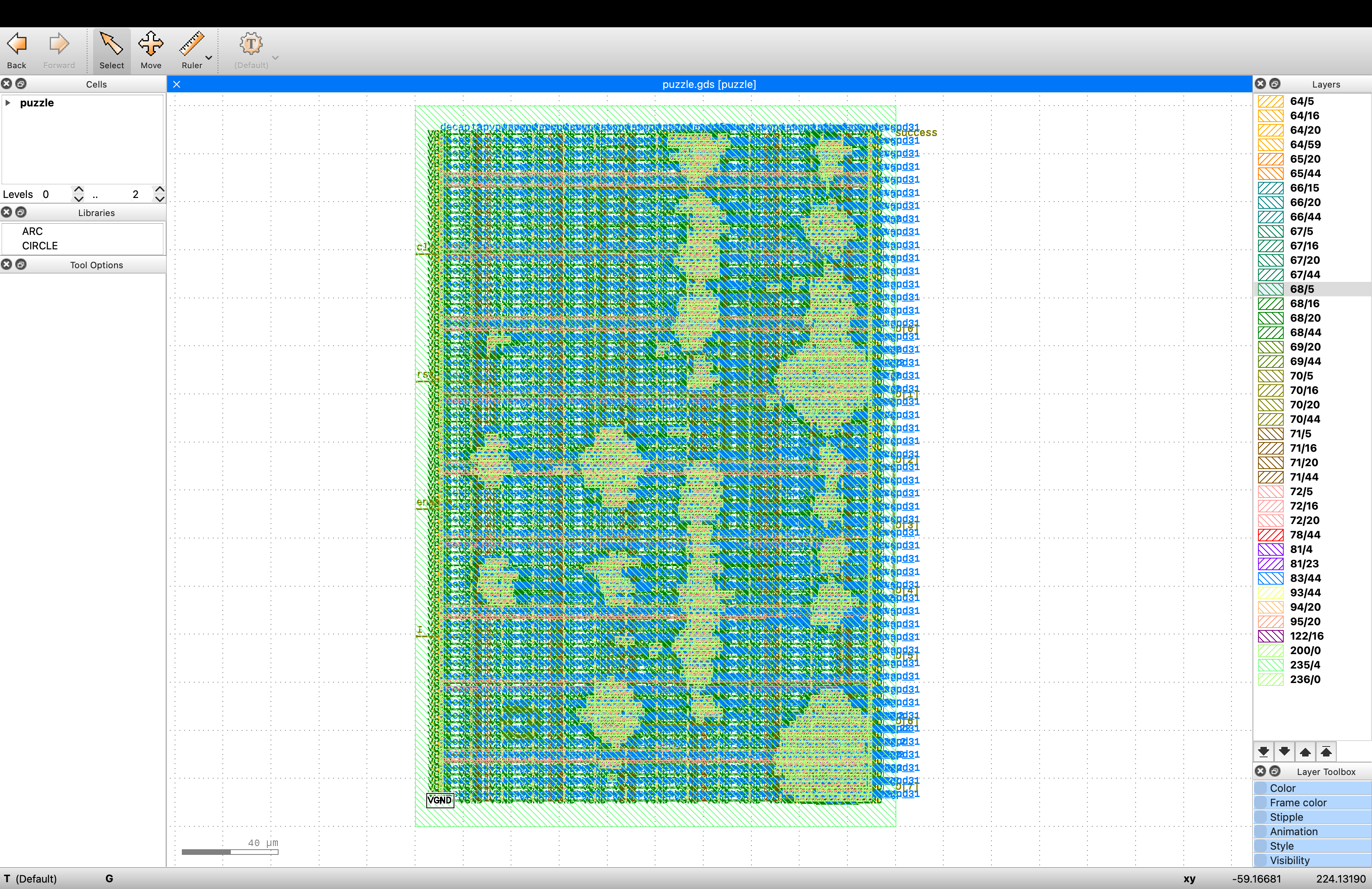
The really, really short answer is that the .gds file describes the physical layout of the chip. More precisely, GDS stores the shapes used to manufacture that physical chip. As a deliberately simplified mental model, you can picture a chip as a stack of layers, where each layer is a set of 2D polygons sitting on a plane.
- You start with a base of silicon on the bottom,
- and then you deposit a horizontal layer of metal (
metal1), - and then you set down some vertical pillars of metal (
via1), - and then deposit another horizontal layer of metal (
metal2), - and then repeat this over and over, each new layer stacked on top of the one below, in this metal 1, via 1, metal 2, via 2, metal 3, via 3, metal 4, ... sort of pattern.
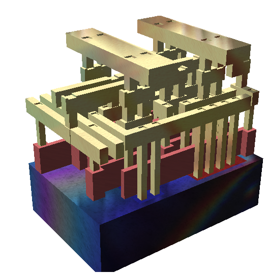 Figure taken from Wikipedia, not the 3D rendering of the puzzle.
Chip designers save the final layout in a file format known as GDSII, which describes the polygons on numbered layers, such that we can render it into the rainbow polygon soup we see in KLayout.
Aside: How Do The Logic Gates....... Become Polygon Soup?
Prior to looking at the contents of the GDS file with gdstk, I assumed I was supposed to learn a bunch of semiconductor physics to understand how the logic gates are compiled into stacks of vertical-and-horizontal metal.
While it turns out we don't need semiconductor physics to solve this challenge, the question of how the logic gates translate into stacks of vertical-and-horizontal metal is interesting nonetheless.
Basically, logic gates are built from transistors, which are electrical switches.
The bottom silicon layer (in indigo) can be thought of as in charge of determining what transistors exist; it is "doped" in such a way that current can flow through some parts of the silicon but not others, and each transistor's "gate" switches its current on or off.
The upper layers on top of the silicon (in red and yellow), i.e. the metal1-via1-metal2-via2... layers, can be thought of as in charge of wiring the transistors together to create the logic gates NAND/NOT/NOR/etc.
If you're curious, SiliWiz goes into how a gate is manufactured - you quite literally draw shapes on top of each other and run the simulation for resistance and such. Thank you to the challenge author / my CMU friend Anish for recommending this resource!
Chip Design Process
Great, we have this polygon soup, but we want to get it into a higher-level, more easily understandable format. To understand what formats we're aiming for, we must learn a little more about the chip design process.
In chip design, the flow is normally:
- You describe the circuits in a hardware-description language (HDL) like Verilog (
.v,.vh) - The HDL gets compiled down into logic gates, producing a description known as a gate netlist. This process is known by hardware folks as "synthesis".
- The gate netlist is then placed-and-routed into a physical layout (
.gds).
A Little Terminology
For the purposes of this post, an electrical component can be thought of as a bunch of pins, some of which are input pins and some are output pins.
A net is one electrical wire, which can be thought of as the set of pins that are all tied together.
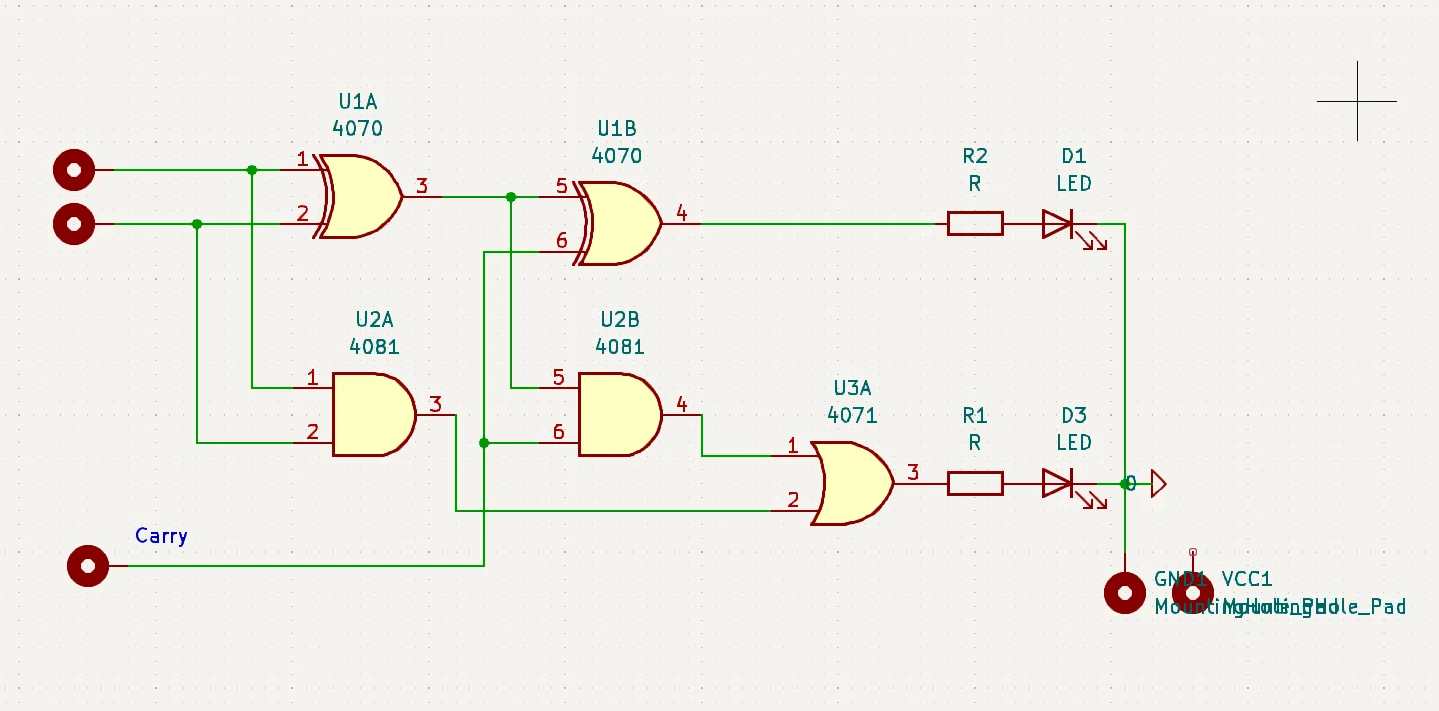
A netlist is the list of every component alongside how they're connected together, in the form of which nets touch each of their pins. When the components in that list are logic gates and not something lower-level or higher-level than that, we call it a gate netlist.
Contextualized in the image below, the components are the yellow shapes with red outlines, and the nets, aka connections between components, are in green.
So it would be sensible to suggest that we go backwards:
- From the physical layout, we want to identify standard-cell placements and the metal connections between their pins.
- We reconstruct the gate netlist by looking up each named standard cell's behavior and recording which recovered net touches each pin.
- We analyze the circuit that is represented by these logic gates and look for the magical input string that'll make its success signal go high.
Steps 1 and 2: Deriving a Circuit Reconstructor from the Warm-Up Puzzle
Thankfully, the puzzle authors provide us with a warm-up puzzle, so we can practice the circuit reconstruction process on a smaller, more digestible polygon soup before we move on to the meatier puzzle.gds.
A pretty reasonable flow is to compare the gate netlist of the warm-up puzzle (01_netlist.v), its post-route connectivity (03_post_place_and_route.def), and its physical layout (04_final.gds) to learn how logic gates and wires are represented in polygon soup.
From these learnings, we can write a GDS-to-netlist extractor and refine it until every recovered warm-up net has the same set of instance pins as the post-route connectivity .def. Comparing sets of endpoints is more useful than comparing text because the final GDS no longer retains the original signal-net names. When the recovered connectivity matches that in the warm-up puzzle, we can reuse the same extractor on the actual puzzle.
Finally, from the recovered connectivity, we generate a gate-level Verilog circuit by assigning each SKY130 cell its known behavior and connecting them through their recovered nets. Those shared nets implicitly describe which gates depend on which other gates, and tools such as Icarus and Yosys derive the dependency graph automatically.
Writing the Netlist Extractor
Using gdstk, I began by dumping the top-level labels and hierarchical cell references from the GDS. The important references fell into two categories:
- First are vias, which connect conductor layers (see vertical pillars in 3D diagram), prefixed with
VIA_, likeVIA_M1M2_PR. - Second are SKY130 library-cell placements (see horizontal structures in 3D diagram), prefixed with
sky130_fd_sc_hd__, likesky130_fd_sc_hd__mux2_1orsky130_fd_sc_hd__clkbuf_16. Some are logic cells (think logic gates), while others are for physical/manufacturing reasons only and can be excluded from the netlist.
There was also a third type of label, prefixed by INTERNAL_, that is part of Easter Egg 1 and unrelated to the function of the chip. We will talk more about this in the Easter Eggs section!
Intuitively, we can think of the .gds file as a graph, where each polygon is a node, and an edge joins two polygons whenever they're electrically connected, either because:
- case 1: they overlap on the same layer, or
- case 2: a via bridges them between two different layers.
So loosely, to obtain our netlist, the algorithm we want to write uses geometric union plus a union-find:
Algorithm 1: Union-Find for Netlist Extraction
- Begin with each polygon in its own set.
- For each layer, merge touching or overlapping conductor polygons independently on each layer. More precisely, each merged conductor component is
union'd into its own set.- For each via,
unionthe component onmetal-Nwith the component it touches onmetal-N+1.After running this union-find algorithm, each disjoint set is one net.
To determine which gates have dependencies on each other, we do the following:
Algorithm 2: Reconstructing a Gate-Level Model
- Acquire the netlist by running Algorithm 1: Union-Find for Netlist Extraction.
- For each cell pin, identify which net it is on. You can do this by transforming its coordinates relative to the cell into coordinates relative to the whole chip, and identify which net contains those coordinates.
- Annotate each pin with its direction (input/output) and whether boolean/sequential based on the SKY130 library data.
- For every recovered cell, emit a Verilog representation of the gate and specify which recovered wire connects to each pin. Check for suspicious wires with no source or multiple sources.
After running this algorithm, we have a model of the chip’s gates and wiring between gates that can be simulated, even though we have not identified the higher-level purpose of every group of gates.
AI Note
I most definitely used AI in writing the extractor. When it comes to AI-generated code, I believe it's more informative to give the prompts that produced the code than the code itself, which tends to be verbose and harder to read. I basically gave Codex the English description of the two algorithms above, that we desired to have a Verilog netlist by the end of the process, and told it to validate against the warm-up puzzle.
Algorithm 1: Union-Find for Netlist Extraction
To walk through a simple example, when we inspect this via that connects metal1 to metal2:
via = next(
    ref for ref in top.references
    if ref.cell.name == "VIA_M1M2_PR"
    and abs(ref.origin[0] - 48.07) < 1e-6
    and abs(ref.origin[1] - 70.21) < 1e-6
)
print(via.origin)
print(sorted((p.layer, p.datatype) for p in via.cell.polygons))
...we get:
origin: (48.07, 70.21)
child geometry: (68,20), (68,44), (69,20)
Based on the child geometry, we see that conductor enclosures are connected on GDS layers 68 and 69. So, according to our union-find algorithm, we find the metal-1 and metal-2 conductor components containing the via origin and union those two component sets.
Algorithm 2: Reconstructing a Gate-Level Model
Codex was especially helpful for resolving the nets of pins, by applying the rotations and transformations that I otherwise would've had to debug by hand.
Take the multiplexer as an example. We want the pins map, which tells us which net each pin is attached to.
{
  "name": "sr_b/_11_",
  "cell": "sky130_fd_sc_hd__mux2_1",
  "origin": [34.04, 21.76],
  "pins": {
    "A0": "net_0021",
    "A1": "net_0015",
    "S": "net_0004",
    "X": "net_0079"
  }
}
But the cell only gives us each pin's local offset, relative to the cell's own origin:
mux = next(c for c in lib.cells if c.name == "sky130_fd_sc_hd__mux2_1")
for label in mux.labels:
    if label.layer == 67 and label.texttype == 5:
        print(label.text, label.origin)
This prints e.g. A0 at (2.075, 1.190), which is not where the pin sits on the chip!! Luckily, from the GDS reference we already know the component's origin (which is where the component resides on the chip) and its rotation (here, it's R180, aka 180 degrees or pi radians).
So we ask Codex to write the extractor such that we derive each pin's global position from its local offset, the origin, and the rotation. For R180, that means negating the offset and adding the origin, i.e. (34.04 - 2.075, 21.76 - 1.190) = (31.965, 20.570), then reading off the net at that point.
Validating Correctness of Logical Circuit
There are two different things that we need to validate:
- Did we recover the right wires (aka netlist) from the GDS?
- Did we assign the right behavior to the cells connected by those wires?
Q1: "Just" compare our netlist with 01_netlist.v? Not quite! We compare by endpoints.
For the first question, I know what you might be thinking, but a simple comparison against 01_netlist.v would NOT work very well because the final GDS has lost most of the original net names. Our extractor calls them things like net_0021, whereas the synthesized netlist may call the same wire something different.
Instead, we use 03_post_place_and_route.def, which retains the original instance names and the set of instance pins belonging to every routed net.
We compare each recovered net by its set of endpoints, where an endpoint is either a top-level chip port or a pin on a standard cell. The names we assign to the nets do not matter. For example, if one net in the DEF connects the top-level port to the S pin of all 16 multiplexers, the recovered connectivity must contain a net with that same set of endpoints.
Our first attempts revealed that Codex made two kinds of extraction errors, one being incorrect endpoint positions for reflected/rotated cells, and the other being standard-cell pins that could be reached through more than one legal metal access shape. After prompting Codex to address those problems, the extractor recovered 84 endpoint groups, where all 84 of these endpoint groups matched the corresponding groups in 03_post_place_and_route.def.
Q2: Did we assign the right behavior?
For the second question, we generate a Verilog model from our netlist and compare its behavior with the original 00_source.v. We write a testbench that shifts all 65,536 possible pairs of eight-bit register values into both designs and compare their outputs. The test bench passed all comparisons.
When we look at the two example failing inputs in example_inputs.vcd, we see that the circuit emits TRY AGAIN for those two inputs. We confirm that our model emits TRY AGAIN too for those same two inputs, albeit one clock edge earlier than seen in the VCD. In spite of being one clock edge earlier, this doesn't affect our ability to recover the target string from the circuit :P
Step 3: Final Boss, Solving the Circuit With SAT-Solver
Okay, great, we wrote our circuit reconstructor, and we validated that it works on our warm-up puzzle!
Now we've run this reconstructor on the actual puzzle and have a Verilog model of the puzzle chip.
The remaining task is to find the input bits, aka values to set the I signal at each clock cycle, that make success go high.
Sure, we can manually work backward through hundreds of gates and oodles of registers, using our human brains to thinky think and assign a human purpose to every internal block, but... I don't know about you, my brain is kind of tired today.
Instead, we can use the fact that our reconstructed Verilog already describes exactly how all those pieces behave and ask a SAT solver to search it.
A Primer on SAT Solvers
In short, SAT is short for "boolean (SAT)isfiability", and a SAT solver answers a question of this form:
Given a collection of boolean rules, is there some choice of true/false values that makes all of these boolean rules true at once?
In some sense, our circuit of logic gates is already a collection of boolean rules. An AND gate is the equivalent of the rule X = A & B, while a multiplexer is the equivalent of the rule X = S ? A1 : A0, and so on.
What's more, Yosys has a built-in SAT solver that can translate our generated Verilog into these boolean rules.
Because our circuit is stateful, we give Yosys a finite number of steps to search. The Yosys sat -seq 140 command makes 140 copies of our circuit's state-transition rules, connects the state after one step to the state before the next step, and lets the circuit's input bit I be a value chosen by the solver at each step.
For constraints, we constrain the circuit to things we know, such as
- we assert reset on the first step and release it afterward,
- we must keep
enablehigh during the input window and low during output, - we must require all primary inputs to be ordinary zeroes or ones rather than unknown values,
- we must require success to be high at the step where the circuit begins producing its output.
We write those requirements as a Yosys .ys command file, then we run Yosys, which reads and flattens the Verilog, converts it into formal state logic, and its built-in sat command does the SAT-solver magic of bounded search.
If no input sequence can satisfy those rules, Yosys returns with the result UNSAT. If at least one input sequence can, the result is SAT, and Yosys prints a witness, aka one sequence of input bits and accompanying signals that can solve the circuit.
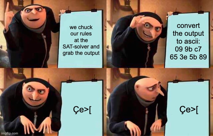
Note that there exist many witnesses, and not all witnesses produce the desired result. Our first query to Yosys' SAT solver required only success=1. It did find a witness quickly, but the corresponding output was mostly non-ASCII.
Hmm!
We need to add a constraint to our SAT-solver that is related to the readability of the output string. Since the puzzle asks us to recover a readable string, we added one more constraint to the harness, which is that all characters in the output must be printable ASCII, with printable defined as...
assign printable = O >= 8'h20 && O <= 8'h7e;
After requiring all 15 output bytes to be printable ASCII, Yosys then finds a successful witness whose output bytes are:
28 2a 20 54 57 4f 20 53 54 41 52 53 20 2a 29
Those bytes decode to:
(* TWO STARS *)
which is the answer we submit to the submissions form.
Boy or Girl? It's a Star Battle checker!!
So, the purpose of the chip, aside from being a puzzle... drumroll... is to be a checker for the two-star Star Battle game!
After I googled "games with two stars" and went down the search results, this result seemed most plausible -> Star Battle
We can confirm this is a Star Battle checker by looking at the input string. When we reshape our successful input on an 11x11 grid (guessing based off of 121 being a perfect square) and we interpret each high-signal as a star, there's two stars per row and column.
     .*........*
     ....*.*....
     *.......*..
     ...*.*.....
     .......*.*.
     .*.*.......
     .....*..*..
     ..*.......*
     *.....*....
     ....*....*.
     ..*....*...
Addendum: Easter Eggs
I found three easter eggs in the solving of this challenge, that I'm fairly convinced are intentional due to following the star theme:
Easter Egg 1: PER ARENAM AD ASTRA
When you throw the GDS file into KLayout, you immediately see this weird row of green rectangles that doesn't seem to be part of the chip.
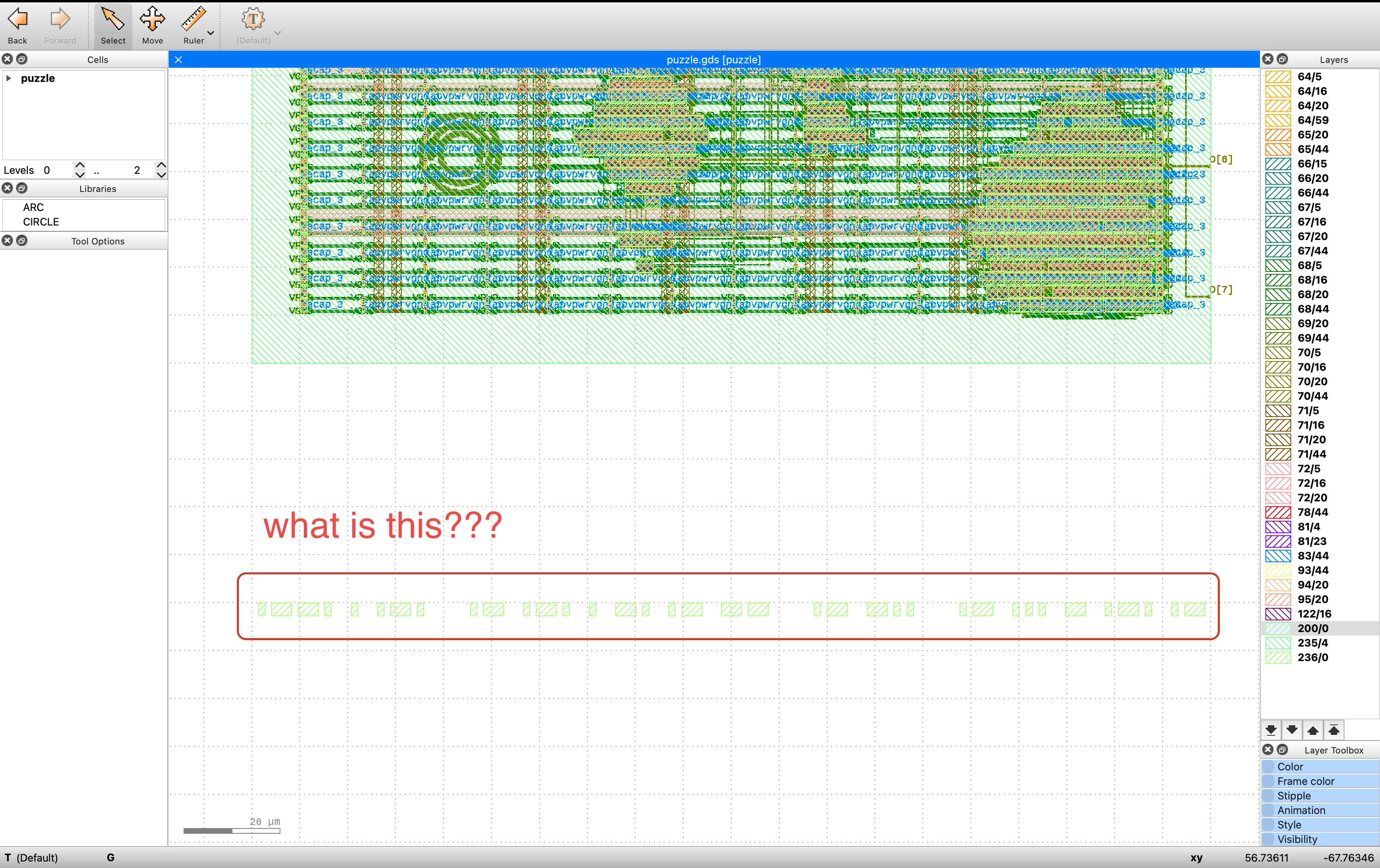
We can attribute these rectangles to layer 200, and layer 200 is weird. Its rectangles are arranged neatly in one row, with exactly two types of rectangles, one of a super short width and one of a longer width, 3x wider to be exact.
3x wider, that sounds familiar! In Morse code, the dot is one time unit long and the dash is three time units long, so this could be Morse code.
Decoding the rectangle in Morse code, we get "PER ARENAM AD ASTRA".
Easter Egg 2: "The night sky awaits"
Here, we take the hint in example_inputs.vcd, "Leave no stone unturned!" and look at the file in the waveform viewer.
When we record the value of the I signal for every rising clock edge where enable is high and ASCII-decode these recorded bits, we get "The night s" and "ky awaits".
Easter Egg 3: Leap Second
The date in the vcd is Sat Dec 31 23:59:60 2016, which is far far before this puzzle was made. According to Wikipedia, this is a leap second, and the most recent one, in fact! So TIL that leap seconds are a thing. :)
Conclusions
This is the lowest on the stack I've gone for reverse engineering.
The biggest surprise for me was that going lower on the stack did not mean I had to understand transistor physics or manually understand every gate. Thank you SkyWater Technology for publishing the SKY130 standard-cell library which already names each gate and tells me the behavior of each sky130_fd_sc_hd__ thingo. And thank you Yosys SAT solver for sparing me from needing to reverse engineer the purpose of every group of gates.
And thank you, challenge authors, for bringing us this puzzle and showing me that the chip-design stack is more approachable than I initially thought.